Presently, a new transmission electron microscope is being installed at the KIT Laboratory for Electron Microscopy. Funding of EUR 4.2 million was provided within the excellence initiative. The KIT southern campus is the first university in Germany that will conduct research with a FEI Titan3 80-300 “Cubed”. In Germany, only the Leibniz Institute for Solid-state and Materials Research, Dresden, has another instrument of this type. Worldwide, only about ten instruments exist.

Valuable heavy load: The transmission electron microscope moves into the KIT’s CFN building.
(Photo by: G. Zachmann)

Key component of the microscope: Assembly of the electron source.
(Photo by: Levin Dieterle)
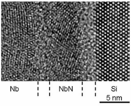
The transmission electron microscope weighs six tons. “With its resolution of 0.08 nm (1 nm corresponds to 0.000000001 m), individual atoms become well visible and it is even possible to image their movements on surfaces”, underlines Professor Dagmar Gerthsen, head of the KIT Laboratory for Electron Microscopy. The KIT scientists will use the new microscope for structural analysis in many areas, for instance in materials research, nanotechnology, solid-state physics, chemistry, and even biology. Up to 30 institutes will profit from the new microscope. “Transmission electron microscopy has the unique feature of analyzing not only the structure, but also the chemical composition and electronic properties of nanometer-sized sample areas”, says Gerthsen. An example are quantum dots which are used in semiconductor lasers. The chemical composition of the quantum dots may vary on the atomic scale from atomic layer to atomic layer and cannot be controlled precisely during fabrication. It is therefore necessary to analyze it in the object.
Interest of materials researchers focuses, for instance, on the enrichment of impurity atoms at grain boundaries. These are the areas between differently oriented grains of the material. Impurity atoms may adversely affect the strength of materials inducing even component failure. KIT scientists will now be able to visualize and chemically analyze these impurities with the new microscope.
The microscope can also be used to study causes of the decreasing performance of fuel cells. Here, research focuses on chemical reactions between electrodes and solid electrolyte material as well as on decomposition processes in the electrolyte. As a result of such processes, chemical compositions may vary on the scale of a few nanometers only.
Another field of use of the new microscope is the analysis of the structure and chemical composition of novel functional nanoparticles and molecular structures that can be used in the medical sector as drug containers or electronic components in the future.
Holography in the transmission electron microscope allows to visualize on a nanometer scale electric fields in the vicinity of defects in semiconductors that reduce the mobility of charge carriers in semiconductor devices. Presently, technicians are still adjusting the new microscope. “From February, we will be able to fully use it”, underlines Dagmar Gerthsen.
The Karlsruhe Institute of Technology (KIT) is the merger of the Forschungszentrum Karlsruhe, member of the Helmholtz Association, and the Universität Karlsruhe. This merger will give rise to an institution of internationally excellent research and teaching in natural and engineering sciences. In total, the KIT has 8000 employees and an annual budget of 700 million Euros. The KIT focuses on the knowledge triangle of research – teaching – innovation.
The Karlsruhe institution is a leading European energy research center and plays a visible role in nanosciences worldwide. KIT sets new standards in teaching and promotion of young scientists and attracts top scientists from all over the world. Moreover, KIT is a leading innovation partner of industry.

