
New Imaging Technique with 3D-printed Nanolenses
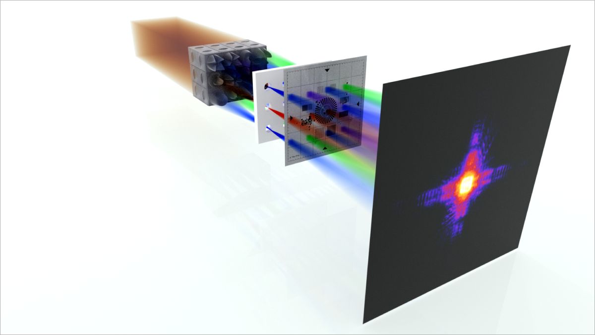
A new X-ray imaging technique can visualize the internal structure of much larger samples than previously possible, with nanometer resolution and without damaging them. Researchers at the German Electron Synchrotron (DESY) have developed the so-called multibeam ptychography with significant expertise from the Karlsruhe Institute of Technology (KIT). The newly developed technology enables the analysis of entire microchips or catalyst particles, for example to optimize their processes.
"A level never achieved before"
In the experiments, the scientists improved the imaging by a factor 12. They scanned the samples with extreme precision of 38 nanometers within ten minutes. "In terms of high-resolution measurements at high speed, this technology takes 3D visualization to a level never achieved before," says Dr. Thomas Sheppard of the Institute of Technical Chemistry and Polymer Chemistry at KIT, assessing the development. This will be of particular interest for catalysis research, material design and the microelectronics industry.
In addition to Sheppard, who prepared and contributed some of the microscopic samples, the spin-off Nanoscribe, founded by Professor Martin Wegener of the KIT Institute of Applied Physics, was also crucially involved in the new technology. Nanoscribe developed the nanolenses for the process using a high-resolution 3D printer. Densely packed and supported by intelligent algorithms, they form a grid that better captures the X-rays generated by the electron synchrotron, thereby better illuminating the sample.
iha, July 22, 2024